In semiconductor equipment, a plastic part is rarely “just a plastic part.”
It may be a small spacer inside a module. It may be a wafer handling guide, a sensor holder, an insulating block, a wear pad, or a custom replacement part for an older tool. The geometry may look simple, but the working environment is usually not simple at all.
Heat, chemicals, friction, vacuum conditions, repeated cleaning, tight alignment, and contamination control can quickly expose the weakness of ordinary plastics. A material that works well in general industrial equipment may creep, wear, outgas, deform, crack, or generate particles when it is placed inside a semiconductor process tool.
That is why engineers often consider custom PEEK and Vespel parts when standard plastics are no longer reliable enough.
PEEK is often selected when the part needs a strong balance of mechanical strength, chemical resistance, electrical insulation, and CNC machinability. Vespel® is usually considered when the requirement becomes more demanding: higher temperature, sliding wear, vacuum stability, low particle risk, or better long-term dimensional control.
For many semiconductor projects, these parts are not high-volume molded products. They are custom machined prototypes, maintenance parts, engineering test parts, or low-volume precision components. That makes PEEK CNC machining and plastic CNC machining practical choices.
PEEK and Vespel Are Chosen for Different Reasons
PEEK and Vespel are sometimes mentioned together, but they should not be treated as the same material.
PEEK is a high-performance thermoplastic. It is strong, stable, chemically resistant, electrically insulating, and easier to machine than many ultra-high-performance plastics. It is often a good first choice when a semiconductor part needs performance but still has to stay reasonable in cost.
Vespel is a polyimide material family used in harsher applications. It is much more expensive, but it can be the better choice for wear parts, vacuum-related parts, high-temperature zones, sliding contact areas, and precision components where failure or contamination would be very costly.
A simple way to think about the choice:
| Requirement | PEEK Is Often Suitable When… | Vespel Is Often Considered When… |
|---|---|---|
| Cost control | The part needs high performance but cost still matters | Material cost is secondary to reliability |
| Temperature | Heat resistance is needed, but not extreme | Higher thermal stability is required |
| Wear | Light to moderate wear is expected | Sliding wear or long service life is critical |
| Vacuum / outgassing | Application allows a suitable PEEK grade | Low outgassing is a major concern |
| Machining risk | Precision features are needed at manageable cost | The part is critical enough to justify premium stock |
| Typical parts | Insulators, holders, fixtures, spacers | Bushings, wear pads, wafer contact parts, guides |
The best material depends on the actual environment. A static insulator and a sliding wear pad should not automatically use the same plastic.
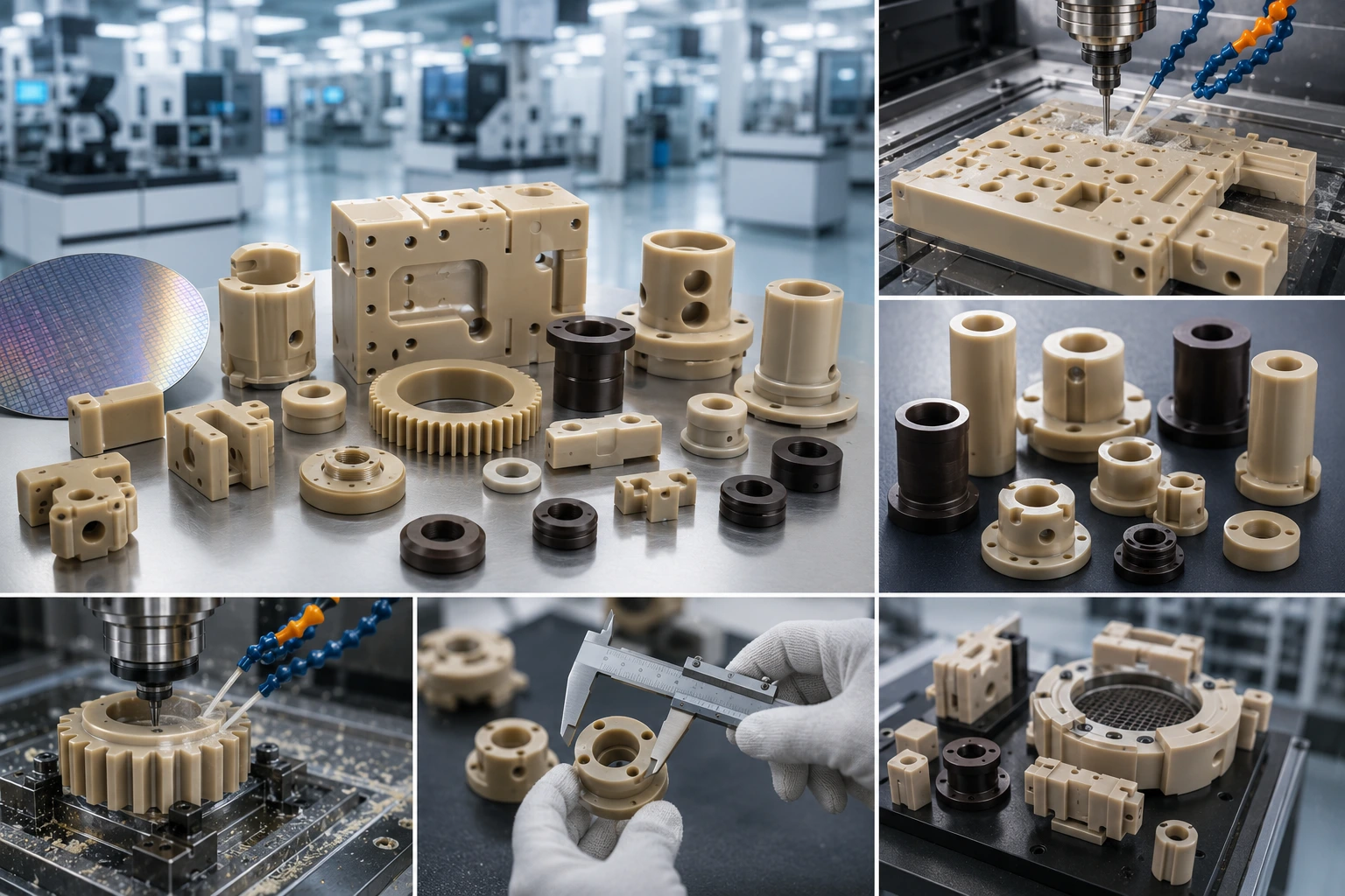
Common PEEK Parts in Semiconductor Equipment
PEEK is often used where metal would create problems: electrical conductivity, chemical reaction, weight, scratching, or contamination concerns.
In semiconductor tools, PEEK parts for semiconductor equipment may include:
- insulating blocks
- spacers and standoffs
- sensor holders
- wafer-related support fixtures
- chemical-resistant brackets
- positioning blocks
- test sockets and connector bodies
- light-duty bushings and guides
- custom maintenance fixtures
PEEK is especially useful when the part needs to be strong enough for assembly, stable enough for precision fit, and non-metallic for electrical or contamination reasons.
But PEEK is still expensive compared with common plastics. If a part has thin walls, long slots, small holes, or tight flatness requirements, the machining plan matters. A poorly planned setup can waste material quickly.
For PEEK CNC machining for semiconductor components, it is better to review the drawing before cutting stock. Sometimes a small radius change, thicker wall, larger screw size, or clearer tolerance note can reduce both cost and risk.
Common Vespel Parts in Semiconductor Tools
Vespel is not usually selected for a simple plastic cover or a basic spacer. The material cost is too high for that kind of use.
It makes more sense when the part has a demanding function: sliding, guiding, insulating, holding position at temperature, or working in a vacuum-sensitive area.
Common Vespel parts for semiconductor equipment include:
- wear pads
- precision bushings
- wafer contact components
- vacuum-compatible spacers
- high-temperature guides
- thermal isolation parts
- small rollers or sliding supports
- custom replacement parts for critical tools
For these parts, the real value of Vespel is not only “it can take heat.” The value is stable performance in difficult conditions. Less wear, less movement, better dimensional control, and reduced failure risk can matter more than the raw material price.
That said, Vespel should not be specified casually. If PEEK is good enough for the job, PEEK may be the more practical choice. If the part is in a high-wear, high-temperature, or vacuum-critical location, then Vespel may justify the cost.
CNC Machining Makes Sense for Custom Semiconductor Plastic Parts
Many semiconductor equipment parts are low-volume by nature. A factory may need 2 pieces for testing, 10 pieces for maintenance, or 50 pieces for a tool upgrade. It may also need a replacement part for equipment that is no longer easy to source.
In these cases, mold tooling is usually unnecessary. CNC machining from PEEK or Vespel stock is faster and more flexible.
With custom CNC machining services, engineers can produce real-material parts with holes, pockets, threads, slots, shoulders, contact faces, and alignment features. If the design needs a revision, the CAD file can be updated without rebuilding a mold.
This is especially useful for:
- custom wafer handling fixtures
- precision plastic insulators
- low-volume replacement parts
- semiconductor maintenance tooling
- equipment upgrade components
- engineering validation parts
- non-metallic brackets and holders
- clean assembly support parts
For tight fit and multi-face geometry, precision machining becomes important because every setup can affect hole location, parallelism, flatness, and final assembly fit.
The Hard Part Is Not Cutting Plastic. It Is Controlling the Details.
PEEK and Vespel do not machine like aluminum or stainless steel. They also do not behave like cheap plastic blocks.
The challenge is control.
Too much clamping pressure can distort a thin plastic part. A dull tool can leave burrs. Heavy material removal can release stress. Small holes can change size if heat builds up. Large flat parts may move slightly after they are removed from the fixture.
These issues matter more in semiconductor work because the part may need to fit into an existing tool with little room for adjustment.
Typical risks include:
| Machining Risk | Why It Matters |
| Burrs around holes | Can affect clean assembly and particle control |
| Thin-wall deflection | Can change fit after unclamping |
| Warpage | Can affect flatness and alignment |
| Surface scratches | Can be unacceptable on contact or sliding areas |
| Thread wear | Plastic threads may fail after repeated assembly |
| Hole position drift | Can create assembly issues in tight modules |
| Material waste | PEEK is expensive; Vespel is even more expensive |
This is why semiconductor equipment plastic components should be reviewed as precision parts, even when the shape looks simple.
Tolerances Should Be Tight Only Where They Matter
A common mistake is applying tight tolerance across the whole drawing.
For metal parts, that already increases cost. For PEEK and Vespel, it can increase cost and risk even more. Plastic parts respond to heat, stress, clamping, and material removal differently from metal parts.
A better drawing separates critical features from general features.
For example, a wafer contact edge may need a controlled surface and burr-free condition. A mounting hole pattern may need accurate position. A non-contact outer profile may not need the same level of control. A flat seating face may need flatness, but an internal clearance pocket may not.
A practical drawing should clearly mark:
- critical hole diameters
- hole position tolerances
- flatness requirements
- parallelism requirements
- burr-free edges
- wafer contact surfaces
- sliding surfaces
- threaded features
- cleaning or packaging notes
For semiconductor parts, “good finish” is too vague. If the surface touches a wafer, slides against another part, or sits inside a clean module, say that clearly.
Boona’s quality control page fits this kind of work because these parts often need more than a quick size check. Hole size, flatness, edge quality, surface condition, and material verification may all matter.
Clean Edges Are Not Just Cosmetic
In general machinery, a small burr may be annoying. In semiconductor equipment, a burr can be a real problem.
A loose edge, sharp shaving, or rough hole can become a particle source. A scratched contact surface can affect handling. A poorly finished sliding part can wear faster. A dirty component can create problems even if the dimensions are correct.
That is why precision plastic parts for semiconductor tools often need controlled deburring and cleaning.
For PEEK and Vespel parts, the goal is not aggressive polishing. The goal is clean, controlled edges without damaging precision features.
Good manufacturing notes may include:
- burr-free holes
- no loose chips or debris
- smooth wafer contact edges
- no aggressive rounding on critical surfaces
- protected sliding faces
- clean packaging required
- avoid scratches on functional surfaces
If special cleanliness is required, it should be written in the RFQ. Standard shop cleaning and semiconductor cleanroom-level handling are not the same thing.
For edge and finish planning, surface finishing guidance can help define what is realistic before production.
Material Grade Should Be Confirmed Before Quoting
“PEEK” is not always enough information. “Vespel” is not always enough either.
PEEK can be natural, black, glass-filled, carbon-filled, or bearing grade. Vespel also has different grades designed for different combinations of wear, temperature, vacuum, insulation, or mechanical performance.
If the grade is not confirmed, the quote may be incomplete or inaccurate.
A good RFQ should include:
| RFQ Detail | Why It Helps |
| Material grade | Avoids wrong stock selection |
| Operating temperature | Helps confirm material suitability |
| Chemical exposure | Prevents material compatibility problems |
| Vacuum requirement | Helps review outgassing concerns |
| Wear or sliding condition | Helps decide between PEEK, Vespel, or filled grades |
| Quantity | Affects setup cost and stock planning |
| Critical tolerances | Helps focus inspection on important features |
| Cleanliness requirement | Affects cleaning, handling, and packaging |
| Material certificate | Supports controlled maintenance and traceability |
If the customer does not know the exact grade, the application details become even more important. A supplier can give better feedback when they know how the part will be used.
What Makes These Parts Expensive
PEEK and Vespel parts can be expensive for several reasons. Material cost is only one of them.
Vespel stock can be very costly. PEEK is also much more expensive than common engineering plastics. If the part requires a large blank and most of the material is machined away, material waste becomes a serious cost factor.
But geometry can matter just as much as material. Thin walls, deep pockets, small holes, tight flatness, and strict burr-free requirements all add time. Clean packaging and documentation also increase cost.
Main cost drivers include:
- material grade and stock size
- part quantity
- tight tolerances
- thin walls or weak features
- large flatness requirements
- small holes and fine threads
- controlled deburring
- cleaning and packaging requirements
- inspection report or material certificate
- urgent delivery
The best way to control cost is not to remove quality requirements. It is to define them more clearly. Mark the critical surfaces. Keep general tolerances realistic. Avoid over-specifying features that do not affect function.
For small runs, low-volume manufacturing is often suitable because many semiconductor plastic parts are ordered in low quantities for maintenance, validation, or equipment upgrades.
Better Design Choices for PEEK and Vespel Parts
Good DFM matters more when material is expensive.
A small design improvement can reduce scrap risk and machining time. A larger internal radius may allow a stronger tool. A thicker wall may reduce deflection. A slightly larger thread may improve assembly life. A clearer surface finish callout may prevent unnecessary polishing.
Useful design habits include:
- avoid very thin unsupported walls
- add radii to internal corners
- allow enough tool access for pockets
- avoid unnecessary tight tolerances
- mark wafer-contact or sliding faces clearly
- use inserts for repeated threaded assembly when needed
- specify burr-free edges only where they matter
- define flatness separately from surface finish
- state cleaning and packaging requirements early
For high-value semiconductor components, DFM is not about lowering quality. It is about making the part more reliable to manufacture.
Final Thoughts
Custom PEEK and Vespel parts are used in semiconductor equipment because ordinary plastics often cannot meet the combination of heat resistance, chemical resistance, wear control, insulation, dimensional stability, and cleanliness requirements.
PEEK is often the practical choice when the part needs strong overall performance and reasonable machinability. Vespel is usually reserved for more demanding locations where wear, heat, vacuum stability, or particle control matters more than material cost.
The most successful projects do not start with “machine this plastic part.” They start with a clear understanding of the part’s job: where it is installed, what it touches, how hot it gets, whether it slides, whether it sees chemicals, and which dimensions truly matter.
For engineers sourcing PEEK parts for semiconductor equipment or Vespel parts for semiconductor equipment, a clear drawing and a complete RFQ can prevent rework, reduce scrap, and make the final parts easier to inspect and install.
FAQs
Why are PEEK and Vespel used in semiconductor equipment?
PEEK and Vespel parts are used in semiconductor equipment because they can handle demanding conditions better than ordinary plastics. They offer strong dimensional stability, electrical insulation, wear resistance, and resistance to heat or chemicals. These properties make them useful for insulators, wafer handling fixtures, bushings, guides, spacers, and precision plastic components inside semiconductor tools.
What is the difference between PEEK and Vespel for semiconductor parts?
PEEK is often chosen when a part needs a good balance of strength, chemical resistance, insulation, machinability, and cost control. Vespel is usually selected for more demanding areas where wear resistance, high temperature performance, vacuum stability, or low particle generation is more critical. In simple terms, use PEEK when it meets the requirement, and consider Vespel when the working environment is too severe for PEEK.
Can PEEK and Vespel parts be CNC machined to tight tolerances?
Yes, PEEK CNC machining and Vespel CNC machining can produce high-precision custom parts, but tolerance depends on part geometry, wall thickness, flatness requirements, material grade, and machining setup. Thin walls, deep pockets, large flat surfaces, and small holes need extra attention because high-performance plastics can move, deflect, or show burrs during machining.
What types of custom PEEK parts are common in semiconductor equipment?
Common PEEK parts for semiconductor equipment include insulating blocks, spacers, standoffs, sensor holders, wafer-related fixtures, positioning blocks, chemical-resistant brackets, connector bodies, and light-duty bushings or guides. PEEK is often used when the part needs strength, insulation, chemical resistance, and stable fit without using metal.
What types of custom Vespel parts are used in semiconductor tools?
Common Vespel parts for semiconductor equipment include wear pads, precision bushings, wafer contact parts, vacuum-compatible spacers, high-temperature guides, sliding supports, thermal isolation parts, and custom replacement components. Vespel is usually selected for critical areas where wear, heat, vacuum behavior, or particle control matters more than material cost.
What information should I provide when requesting custom PEEK or Vespel parts?
For a faster and more accurate quote, provide a 3D CAD file, 2D drawing, material grade, quantity, critical tolerances, surface finish requirements, burr-free or cleanliness notes, operating temperature, chemical exposure, vacuum requirements, wear or sliding conditions, and inspection or material certificate needs. It also helps to explain where the part is used inside the semiconductor equipment.