
A counterbore gives a fastener room to sit below a busbar’s surface. It also removes copper near the connection. If the design review considers only bolt clearance, it can overlook the remaining current path and usable contact footprint.
Machining copper busbars adds the most value where EV battery systems need stepped contact pads, accurate terminal patterns, or complex low-volume geometries. Specify those features alongside the copper grade, joint loading, plating, and insulation boundaries. A precision-machined bar still requires validation in its actual assembly.
The central engineering question is where resistance develops. The copper conductor and its terminal joints contribute separately, so increasing bar thickness may leave the decisive interface unchanged.
Where Machining Copper Busbars Adds Value
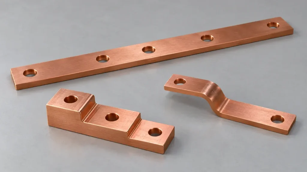
Match the Manufacturing Route to the Geometry
Cell interconnects, module connections, and pack-level distribution bars perform different mechanical jobs. A thin interconnect may need flexibility to accommodate movement. A distribution bar may require rigid terminal pads that locate against contactors or power connectors.
CNC machining suits features that need controlled depth or a defined relationship between surfaces: stepped pads, counterbores, and accurately positioned holes. It also allows design changes without committing immediately to dedicated production tooling.
Uniform flat profiles may suit cutting or punching followed by selective machining. Formed blanks can provide offsets without removing the entire shape from thick stock. Flexible laminated or braided links follow different manufacturing routes and should remain separate options where terminal movement matters.
For component planning, BOONA copper CNC machining service is the relevant starting point. The review should establish which surfaces require machining and which can retain the supplied stock condition.
Specify Copper Grade and Temper Together
The Copper Development Association’s wrought-copper designation table distinguishes C11000 electrolytic tough-pitch copper, C10100 oxygen-free-electronic copper, and C10200 oxygen-free copper. These designations identify different material specifications; “pure copper” leaves the purchasing requirement incomplete.
C11000 is a common high-conductivity starting point. Oxygen-free grades merit consideration when purity or the planned joining process requires them. A substitution should satisfy the electrical and processing requirements of the design, rather than follow a general assumption that every EV busbar needs the highest-purity grade.
Temper matters independently. It affects forming behavior, handling stiffness, and resistance to deformation during clamping. Free-machining grades such as tellurium-bearing C14500 can improve chip behavior, but require approval against the specified conductivity and joining requirements. Include the grade, material condition, and required documentation on the controlled drawing.
Size the Current Path Before Setting Machining Allowances
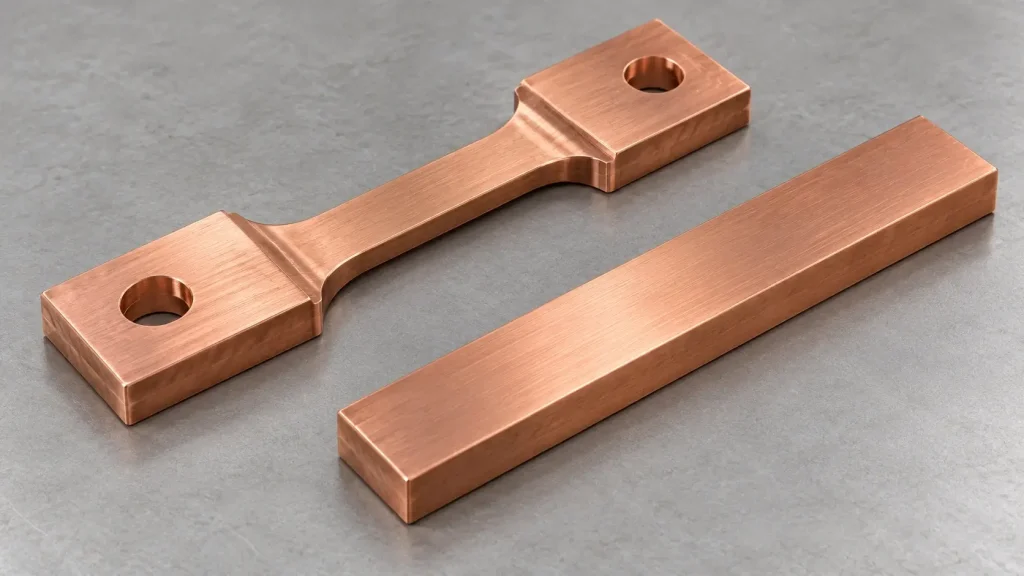
Separate Conductor Losses from Joint Losses
For a uniform conductor, resistance follows R = ρL/A, where ρ is resistivity, L is length, and A is cross-sectional area. Resistive heating follows P = I²R. These relationships help explain why conductor length and section matter, although they do not resolve current distribution around every geometric transition.
A hole interrupts the available section. A counterbore reduces local thickness, while an abrupt neck can concentrate current. Review the remaining conducting geometry around these features instead of sizing from the largest section shown on the drawing.
The joint introduces another resistance contribution. Its performance depends on the actual contacting surfaces and retained clamping load. A wider pad offers room for contact, but its geometric area alone cannot establish how effectively current transfers across the interface.
Define the Operating Conditions
A useful design input distinguishes continuous current from transient duty. It also identifies allowable temperature rise, the surrounding thermal environment, and the cooling arrangement. A bar inside a crowded battery enclosure may reject heat differently from the same bar on an open bench.
Fault-current loading adds mechanical requirements. Supports and terminal connections must withstand the loads established by the system design. Thermal expansion also matters when a rigid bar connects components that move relative to one another.
Avoid treating a single current-density rule as a release criterion. The assembly designer should evaluate conductor geometry and joint losses together under the intended duty. Where a bar bridges moving terminals, consider a flexible connection or another means of accommodating displacement before tightening the machining tolerances.
Control Contact Faces, Holes, and Burrs as One Interface
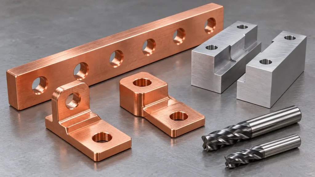
Contact Geometry and Fastener Loading
Define the usable contact footprint separately from the bolt-hole pattern. Hole position controls assembly access and alignment; pad geometry controls how the mating surfaces meet. Specify their relationship through functional datums, with flatness or parallelism requirements where the joint design needs them.
A polished appearance does not establish low contact resistance. Surface films, mating finishes, and contact pressure remain relevant. Likewise, tightening torque is an assembly input whose relationship to preload depends on the fastener stack and friction conditions.
Slots can accommodate positional variation, but may reduce overlap or move the clamping location. Check the joint throughout its permitted adjustment range. For tapped copper features, evaluate thread engagement and service loading against the material condition; approved studs or through-fasteners may be alternatives.
Pro Tip: Dimension the usable electrical contact footprint separately from the fastener hole, and identify where plating or insulation transitions are permitted.
Machining and Deburring Decisions
Copper can adhere to cutting edges and form persistent burrs. Sharp tooling, effective chip evacuation, and suitable support help control the process. Fixture contact should avoid damaging terminal lands or forcing a thin section into a misleading machining position.
For a BOONA DFM review, our decision rule is to protect the contact footprint during deburring. If a chamfer would consume part of that footprint, define the permitted edge break and contact boundary separately. A general instruction to “deburr all edges” gives insufficient control at a narrow terminal land.
If forming changes terminal-pad alignment, our recommendation is to evaluate final pad machining and inspection after forming. Machining both pads accurately beforehand does not establish their final relationship after bending. The drawing should identify the final geometry and its measurement condition.
Remove chips and cutting-fluid residue before finishing. Pay particular attention to blind features and threaded holes, where retained contamination can reach a contact surface during handling or assembly.
Coordinate Plating, Insulation, and Final Dimensions
Select Plating for the Joint Environment
Tin, nickel, and silver finishes serve different interface requirements. Section 1.1 of ASTM B545-22, Standard Specification for Electrodeposited Coatings of Tin, describes electrodeposited tin coatings used to reduce contact resistance, provide corrosion protection, and support soldering. Section 1.2 discusses protection on copper under normal indoor exposure and identifies limitations associated with outdoor exposure, coating discontinuities, and humidity. These statements do not establish suitability for a particular EV battery joint. Evaluate nickel and silver finishes separately against the mating materials, service environment, and joining method. Specify any underlayer, coating thickness range, and required coverage with the finishing supplier.
Treat plating as part of the dimensional plan. Deposited material can affect hole clearance, thread fit, and pad height. Identify whether each critical dimension applies before or after finishing, then agree the necessary machining allowance with the finishing supplier.
Masking introduces boundaries that need explicit control. A coating transition within a contact footprint can change how the joint seats. A location suitable for an electrical contact may be unsuitable for a processing rack mark. Show permitted processing-contact areas on the drawing where they could affect function.
Joining requirements deserve separate review. A finish selected for a bolted connection may require a different approach at a weld zone. Coordinate local coverage with the joining process owner.
Define Insulation Boundaries
Insulating sleeves, coatings, and molded carriers need clean, controlled edges beneath them. Burrs can interfere with coverage or damage insulation during assembly. Define exposed terminal lands and the transition to insulated regions before releasing the part.
The IEC’s “Product detail” section lists the current consolidated IEC 60664-1:2020+AMD1:2025 as Edition 3.1. This standard addresses insulation coordination within its stated equipment scope. Its applicability must be assessed against the battery system’s requirements. It does not independently qualify a supplied busbar or complete EV battery pack.
Clearance and creepage requirements depend on the relevant voltage stresses and environmental conditions, among other design inputs. Specify the assembly requirements rather than copying a universal spacing from an unrelated application. Protective coverage on the bar does not automatically establish the assembled system’s dielectric performance.
Inspect by Function, Then Validate the Joined Assembly
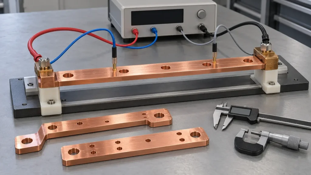
A Feature-to-Verification Matrix
Component inspection should produce evidence for the feature being accepted. Electrical and environmental qualification then assess the actual joined assembly. The following matrix is an engineering review framework, not a set of standardized acceptance grades.
| Functional feature | Component-level evidence | Assembly-level evaluation |
|---|---|---|
| Current-carrying neck | Material identity and net cross-section | Temperature rise under defined duty |
| Terminal contact pad | Geometry, finish, and cleanliness | Joint resistance and stability |
| Fastener interface | Hole location, threads, and finishing allowance | Preload retention and terminal loading |
| Insulation transition | Edge condition, masking, and coverage | Clearance, creepage, and dielectric performance |
| Formed offset | Pad alignment in the specified condition | Movement and loads at connected terminals |
A dimensional report can establish a terminal pattern. It cannot establish resistance after tightening, vibration, or thermal cycling. Keep those responsibilities explicit in the purchase specification.
Measurement setup also influences the evidence. In a 2023 study of planar-contact resistance, Section 3.1.1 and Figure 3(c) in the paper relate probe spacing to modeled current-injection error, reporting contacting error below 0.05% for the recommended spacing under the study’s assumptions.
The research concerned planar conductive-adhesive connections and specimen models, rather than qualification of thick bolted EV busbars. It was not a BOONA project and does not establish BOONA capability. The engineering inference is to fix current-injection and voltage-sense locations when comparing joints, and document any conductor resistance included between the sense points.
Application Example: A Busbar-to-Controller Contact
A 2025 intelligent battery-system study provides an example beyond a conventional terminal-to-terminal bar. Its Abstract describes a research prototype containing 324 automotive lithium-ion cells with a nominal voltage of 400 V.
Section 4.1.1, “Hardware,” describes copper busbars contacting cell-controller circuit boards. The researchers used thick, low-flexibility copper sheets with machined contact surfaces and a large board contact footprint.
For the comparison design, the authors identify seating partly on surrounding solder resist as a possible explanation for higher contact resistance.
Table 3 in that section reports a PCB-to-busbar contact resistance of 4 µΩ. The paragraph introducing the table states that the values are means from five controllers, with an estimated combined measurement error of ±4 µΩ. That uncertainty is the same magnitude as the reported contact resistance.
The study did not isolate machining as the cause of the interface performance. It was a research demonstrator, not a BOONA project or evidence of BOONA capability. The engineering inference is to evaluate the complete contact interface alongside the conductor. These results establish neither a universal resistance target nor automotive qualification.
RFQ Checklist for Machining Copper Busbars
Information Needed Before Quoting
An effective RFQ connects the model to its functional drawing. Supply:
- Copper grade, temper, stock form, and required material documentation.
- Prototype quantities and expected production demand.
- CAD files and a controlled terminal-interface drawing.
- Contact footprints, datums, and critical dimensional requirements.
- Current duty and relevant thermal constraints for engineering review.
- Plating requirements, masking boundaries, and insulation interfaces.
- Forming sequence constraints and final inspection condition.
- Inspection deliverables and responsibility for assembly validation.
For a BOONA RFQ, we recommend identifying terminal contact surfaces directly on the drawing. If the model includes a broad flat region but only a smaller area transfers current, mark that smaller footprint. It gives machining, deburring, and finishing a shared boundary to preserve.
Specify packaging protection for those surfaces as well. A clean contact land needs protection against scratches and contamination through delivery.
Cost Drivers and Route Selection
Compare manufacturing routes on the finished, inspected component. A simple cut blank may require less removal than machining from thick stock, but formed terminal alignment or local pad finishing can add operations.
Small cutters, difficult fixture access, and demanding deburring increase processing effort. Finishing adds preparation and masking requirements. Inspection costs also depend on whether acceptance concerns an individual pad or the relationship between several terminal interfaces.
Selective machining can retain an economical blank while controlling the features that drive assembly performance. Keep tolerance investment concentrated on those features. Tightening every outline dimension does little to resolve an undefined contact footprint or an unspecified finishing condition.
FAQs
Which copper grade is suitable for EV battery busbars?
C11000 is a common high-conductivity option. C10100 or C10200 may suit specified purity or processing requirements. Choose the grade and temper against the electrical, forming, and joining requirements of the actual design.
When should a busbar use CNC machining instead of stamping?
CNC machining suits stepped pads, controlled-depth features, complex prototypes, and changing designs. Simple profiles may favor cutting or stamping, with selective machining where contact geometry requires it. Production quantity alone does not determine the route.
How do holes and counterbores affect current capacity?
They remove conducting material and alter local current distribution. Evaluate the remaining section and temperature behavior around them. The largest width and thickness on the drawing do not describe every local restriction.
Do copper busbars need tin, nickel, or silver plating?
The joint specification determines the need and finish type. Consider mating surfaces, exposure, joining method, and qualification requirements. Plating should also form part of the final dimensional and masking plan.
Which tolerances matter most on electrical contact pads?
Priorities commonly include pad location, flatness, relative height, and the fastener relationship. The joint design determines their limits. Identify the required condition after forming and finishing instead of applying a blanket tight tolerance.
How should busbar joint resistance be validated?
Use a defined low-resistance measurement method, typically four-wire measurement, with controlled probe placement and assembly conditions. Evaluate stability under the application’s relevant loading and environmental tests. Component dimensional inspection alone cannot supply that evidence.
Discuss Your Busbar Drawing with BOONA
Machining copper busbars works best when precision features, contact loading, and finishing requirements share a controlled drawing. Send your CAD files and terminal-interface requirements to BOONA CNC machining team for a free DFM review, with no minimum order quantity. Include the material condition and critical contact boundaries so the review can address manufacturing risks and route selection. Battery-system electrical approval and assembly validation remain separate from supplied-component acceptance.