
“Semiconductor-grade” leaves too much unanswered in CNC machining for semiconductor equipment parts. Consider a chamber lid: its sealing land, process-facing surface, and external mounting pads perform different jobs. Applying one roughness specification and one coating instruction across the entire part can create conflicting requirements for sealing, contamination control, and assembly.
The specification should separate these functions: what each surface touches, which features locate the assembly, and how the finished component will be cleaned and verified.
That approach gives purchasing and manufacturing teams a usable specification. It also helps direct expensive precision work toward the interfaces that affect equipment performance.
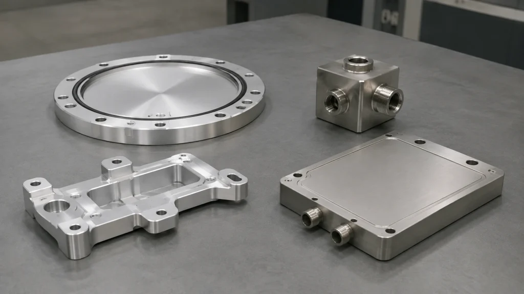
Which Semiconductor Equipment Parts Require CNC Machining?
The equipment category covers a wide range of operating environments. A bracket outside a process chamber faces different demands from a component exposed to vacuum, process gases, or wafer contact.
Process Chambers and Fluid Delivery
Typical semiconductor equipment components include chamber bodies, lids, flanges, gas-distribution plates, valve bodies, and manifold blocks. Their drawings may combine sealing geometry, internal passages, fastening features, and protected process-facing surfaces.
Part classification should establish whether the component serves a structural, vacuum, wetted-fluid, or process-exposed role. This determines which requirements belong in the manufacturing package.
Wafer Handling, Motion, and Thermal Systems
Wafer handling components include robot-interface plates, sensor brackets, and stage supports. Heater mounts and cooling plates add thermal contact and temperature-driven movement to the specification.
The market provides context: SEMI’s April 2026 equipment report records worldwide semiconductor equipment sales of $135.1 billion in 2025, up 15% from 2024. These figures cover manufacturing equipment overall; they should never be presented as the market size for CNC-machined parts alone.
CNC Machining for Semiconductor Equipment Parts: Material Choices
Material selection begins with exposure conditions: process chemistry, temperature, vacuum requirements, electrical behavior, and cleaning compatibility. An alloy name alone cannot establish suitability.
Aluminum and Stainless Steel
6061 aluminum can suit structural plates, thermal components, and selected chamber applications. Specify temper and stock condition because residual stress and subsequent processing can affect dimensional stability.
304L and 316L stainless steels offer alternatives where the approved design requires their mechanical or corrosion characteristics. For high-purity wetted systems, define the material and surface requirements explicitly; commercial stainless stock is insufficient as a complete specification.
| Material family | Potential application | Main selection concern | Drawing or procurement detail |
|---|---|---|---|
| 6061 aluminum | Mounting plates, selected chamber parts | Distortion and process compatibility | Temper, stock condition, finish boundaries |
| 304L or 316L stainless steel | Flanges, valve bodies, manifolds | Chemistry, surface condition, cleanliness | Exact grade and applicable material specification |
| High-purity copper | Thermal interfaces and conductive components | Surface damage, oxidation, contamination | Required purity, condition, protective handling |
| PEEK or PTFE | Selected spacers and insulating components | Creep, temperature, outgassing, additives | Exact grade and approved exposure conditions |
| Alumina or aluminum nitride | Specialized insulating or thermal components | Brittleness and finishing route | Ceramic grade and specialist process approval |
Copper, Engineering Plastics, and Ceramics
Copper, polymers, and ceramics solve different problems. Their inclusion in an equipment assembly does not make them interchangeable substitutes.
Ceramic features may require specialist grinding or other dedicated processes. Confirm the actual manufacturing route and supplier capability before releasing the design.
Planning CNC Machining for Semiconductor Equipment Parts
Semiconductor precision machining depends on relationships between features. A collection of individually tight dimensions can still leave the assembly poorly defined.
Datums, Flatness, and Feature Relationships
Choose datums that represent how the part locates in service. For a chamber lid, the sealing interface and locating features may govern the functional reference system. For a stage support, mounting pads and guide interfaces may matter most.
Separate flatness from parallelism and position. Identify which requirements apply after coating, in the free state, or under a defined assembly condition. These distinctions prevent inspection teams from measuring different interpretations of the same drawing.
Tool Access and Process Selection
Deep pockets, thin walls, and intersecting holes affect tool reach, stiffness, burr formation, and workholding. Add accessible corner radii and avoid unnecessarily long, small-diameter tools.
Five-axis CNC machining for multi-face geometry can help maintain feature relationships while reducing some repositioning steps. It does not automatically improve every part; simpler geometry may suit conventional milling or turning.
Plan roughing and finishing around material removal and clamp loading. Specify only the functional tolerances the design needs, then agree on a measurement method before committing to the machining sequence.
Vacuum Interfaces, Sealing Surfaces, and Internal Passages
Vacuum chamber machining requires attention to both the pressure boundary and the spaces connected to it. A dimensionally correct component can still contain trapped volumes or difficult-to-clean passages.
For sealing interfaces, define the seal type, groove geometry, mating surface condition, and coating exclusions. Surface roughness alone provides an incomplete acceptance rule: scratches crossing the sealing path, burrs, and local damage also deserve explicit inspection criteria.
Blind fastener cavities and overlapping joints can trap gas that escapes slowly into an evacuated space. Review venting with the equipment designer. Any vent must preserve the intended pressure boundary and structural function.
Internal passage intersections deserve particular attention. Provide access for deburring, cleaning, and inspection wherever practical. A drilled cross-hole that saves machining time can introduce additional plugs, interfaces, and verification work.
Leak testing needs its own specification. Identify the test method, assembly condition, pressure differential, acceptance limit, and reporting requirements. Separate an external leak from outgassing or slow gas release from trapped spaces.
The customer and supplier should also agree whether testing covers the individual component, a sealed subassembly, or the completed chamber. Passing one scope does not establish performance at every other level.
Surface Finishing, Cleaning, and Packaging
A finish affects dimensions, chemistry, electrical contact, and subsequent cleaning. Treat it as an engineering operation with acceptance criteria.
Match the Finish to the Surface Function
Review anodizing, electropolishing, passivation, or other treatments against the component’s exposure conditions. These processes perform different functions and should never appear as interchangeable purchase-order options.
Mark masked areas, seal lands, electrical-contact points, and surfaces that require final inspection after treatment. Specify coating thickness or removal allowances where they influence fit. BOONA surface finishing options provide a starting point for discussing available processes; suitability still requires application-specific review.
Control Contamination Through Delivery
Semiconductor parts cleaning must address the contaminants the customer actually controls. Particles, machining-fluid residues, ionic contamination, and organic residues require different assessment methods.
ISO 14644-1’s public scope addresses airborne particle classification. By comparison, ISO 14644-9:2022’s surface-cleanliness scope covers assessment of particles on solid surfaces and explicitly excludes process-specific suitability requirements. A cleanroom designation therefore cannot serve as the complete acceptance specification for a delivered part.
Define cleaning chemistry, rinse and drying controls, verification methods, handling, and packaging together. Prevent packaging materials and inspection activities from reintroducing contamination.
Pro Tip: Review cleaning access before freezing the geometry. A hidden pocket that cannot be inspected or drained becomes a recurring production burden, even when machining it is straightforward.
Inspection and Traceability for Semiconductor Precision Machining
Inspection should answer separate questions about geometry, material, surfaces, cleanliness, and function. One certificate cannot provide evidence for all five.
Dimensional and Functional Verification
Use a drawing-linked inspection plan covering critical datums, sealing features, port positions, and mating surfaces. Select measurement methods that can actually reach the features and resolve the specified tolerances.
A coordinate measuring machine may verify geometry while surface instruments assess texture. Leak, flow, thermal, or cleanliness tests require separate procedures where the purchase specification calls for them.
Record the part’s condition during inspection. A free-state plate, a clamped plate, and a finished assembly can produce different measurements. Temperature and fixture loading can also affect the result.
Documentation and Change Control
The delivery package may include material certificates, dimensional results, finish records, cleaning records, and functional test reports. Agree on the required documents before manufacturing begins.
Tie records to the part number, drawing revision, material lot, and applicable process specifications. Define who approves substitutions and changes involving material, machining, finishing, or external processing.
Finally, sequence inspection and cleaning deliberately. If a part needs additional handling after final cleaning, document how the team will preserve or restore its required cleanliness before packaging.
Application Example: A Magnetic-Levitation Wafer Transfer Platform
A 2023 experimental wafer-handling study from the Korea Institute of Machinery and Materials provides a useful example of how component interfaces support system performance.
The researchers built a platform with a robot above an aluminum base and magnetic-levitation modules at its four corners. Table 2 specifies nominal airgaps of 1 mm in both the x and z directions.
Table 3 reports maximum z-axis fluctuations of ±0.0072 mm at standstill and ±0.101 mm while driving. These are measured system responses, not machining tolerances. Their difference demonstrates why evaluating a stationary assembly alone cannot characterize its behavior during transport.
For the machined supports in a comparable design, the engineering implication is to establish a shared datum structure for mounting and sensor interfaces, then evaluate those relationships under the intended loading and motion conditions. Mass distribution and assembly stiffness deserve attention alongside dimensional inspection.
The paper does not document a CNC process, an aluminum alloy designation, or supplier machining tolerances. It also does not establish a measured particle-removal rate or vacuum-leak performance for this prototype.
This is an independently published equipment-development example, with machining implications drawn as engineering analysis. It is neither a BOONA customer case nor evidence of a production-qualified manufacturing capability.
Preparing an RFQ and Evaluating a Manufacturing Supplier
A useful RFQ allows the supplier to evaluate the complete route from stock to protected delivery. Geometry alone leaves too many cost and acceptance questions open.
Include the controlled 3D model and drawing, exact material specification, quantities, critical interfaces, and required finish. Describe the operating environment sufficiently to identify vacuum, wetted-fluid, thermal, electrical, and process-exposure requirements.
Add the cleaning specification, packaging method, inspection plan, and any functional tests. Identify the standards and revisions that govern acceptance rather than relying on the phrase “semiconductor quality.”
Ask prospective suppliers how they will handle:
- Datum transfer between machining and inspection.
- Burr removal and verification inside intersecting passages.
- Final dimensions after surface treatment.
- Material and process traceability.
- Cleaning, handling, packaging, and outsourced operations.
Separate evidence from assurances. A quality-system certificate does not by itself demonstrate competence for a particular high-purity or vacuum application.
Prototype planning should distinguish fit checks from final qualification. An unfinished sample may answer an assembly question, while approval of the production configuration may require the specified material, finish, cleaning route, and test conditions.
Request a quotation that identifies assumptions, exclusions, and responsibilities for each required operation.
FAQs
What semiconductor equipment parts can be CNC machined?
Examples include chamber lids, flanges, manifold bodies, mounting plates, sensor brackets, and thermal components. The practical scope depends on geometry, material, available processes, and the required finishing and verification route.
Which material is best for semiconductor equipment components?
There is no universal choice. Aluminum, stainless steel, copper, polymers, and ceramics address different structural, thermal, electrical, and chemical requirements. Select the exact grade against the component’s exposure and approved design.
What tolerances do semiconductor parts require?
Use functional requirements to establish tolerances. Sealing surfaces, stage interfaces, and sensor mounts may need different controls. Applying one extremely tight tolerance across the entire drawing can increase cost without improving the relevant performance.
Must semiconductor parts be machined inside a cleanroom?
The customer specification should define environmental controls at each stage. Machining, cleaning, inspection, and final packaging have different contamination risks. A cleanroom label alone does not demonstrate that the delivered component meets its cleanliness limits.
Does every vacuum component need helium leak testing?
Testing depends on the component’s role and purchase requirements. Specify which pressure boundaries or assemblies require testing, the method and limit, and the configuration covered by the report.
What should buyers send with a semiconductor machining RFQ?
Provide the model, controlled drawing, material specification, quantities, finish, cleaning and packaging requirements, inspection scope, and relevant operating conditions. State any customer-approved processes or suppliers that must remain part of the manufacturing route.
Conclusion: Define the Component’s Function Before Manufacturing
CNC Machining for Semiconductor Equipment Parts works best when the specification connects geometry to service conditions. Material choice, datum relationships, surface treatment, cleaning, and verification all influence whether a part is ready for its intended assembly.
Start with the interfaces that matter. Define how they will be machined, measured, treated, and protected. Resolve responsibilities for specialist processing and functional testing before production begins. That preparation gives both the buyer and supplier a clear basis for acceptance and change control.
Send BOONA your CAD model, controlled drawing, material specification, and inspection checklist for a review through its precision CNC machining services. Include the required cleanliness, finishing, packaging, and test conditions so the team can assess the requested scope and identify any qualification needs. BOONA offers no minimum order quantity and a free design-for-manufacturability (DFM) review. Send your CAD to begin the technical discussion.